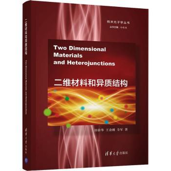
内容简介
本书详细介绍了石墨烯,氮化硼,黑鳞等二维材料,及其它们异质结的合成制备和物理化学质括二维材料的物理制备方法和化学合成的各种方法,详细介绍这些二维材料和它们异质结的物理质括电学,光学,光电,磁学,热学,热电质,以及二位材料超晶格的质。
目录
ConTENTSChapter 1Graphene, Hexagonal Boron Nitride, and Heterostructure:Properties and Applicationr/>1.1Introduction to the 2D materialr/>1.1.1Introduction to graphene1.1.2Introduction to grapheme-like 2D crystals—hexagonal boron nitride 1.1.3Introduction of graphene/h-BN,a 2D composite 1.2Graphene1.2.1Structure of graphene1.2.2Preparation of graphene1.2.3Physical properties of graphene1.2.4Raman spectrum of graphene1.32D h-BN1.3.1Structure of h-BN 1.3.2Preparation of h-BN 1.3.3Physical properties of h-BN 1.3.4Raman spectroscopy of h-BN1.4Composite structure of graphene/h-BN1.4.1Research rise and process of graphene/h-BN heterojunction structure1.4.2Composite mode structure of graphene/h-BN1.4.3Preparations of graphene/h-BN heterostructurer/>1.4.4The properties of graphene/h-BN heterostructurer/>1.4.5Potential applications of graphene/h-BN heterostructure1.5Summary and outlookReferencer/>Chapter 2 Electrical Properties and Recent Electrical Applications of Graphene, h-BN, Graphene/h-BN Heterostructurer/>2.1Graphene2.1.1The structure of 2D graphene2.1.2The electronic structure of graphene2.1.3The electronic property of graphene2.1.4The recent application of graphene in electronic property2.2h-BN2.2.1The structure of 2D h-BN2.2.2The electronic structure of h-BN2.2.3The electronic property of h-BN2.2.4The recent electrical application of h-BN2.3Graphene/h-BN heterostructurer/>2.3.1The structure of graphene/h-BN heterostructurer/>2.3.2The electronic structure of graphene/h-BN heterostructurer/>2.3.3The electronic properties of graphene/h-BN2.3.4The recent application progress of graphene/h-BN heterostructure in electronicr/>2.4Summary and outlookReferencer/>Chapter 3Optical, Photonic and Optoelectronic Properties of Graphene, h-NB and Their Hybrid Materialr/>3.1Introduction to graphene3.1.1Graphene's structure, electronic band3.1.2Electronic properties of graphene, which impact the optical propertier/>3.1.3Optical properties of graphene3.1.4The application of photonics and optoelectronicr/>3.2Introduce of h-BN3.2.1The electronic band structure of 2D h-BN3.2.2The optical properties of h-BN3.2.3Potential applications of h-BN3.3The introduce of graphene/h-BN van der Waals heterostructure3.3.1The structure of graphene/h-BN van der Waals heterostructure3.3.2The energy bandgap structure of graphene/h-BN van der Waals heterostructure3.3.3The optical and photoelectric properties of graphene/h-BN van der Waals heterostructure3.3.4Potential applications of graphene/h-BN heterostructures in optical property3.4Summary and prospectReferencer/>Chapter 4Optoelectronic Properties and Applications of Graphene-based Hybrid Nanomaterials and van der Waals Heterostructure4.1Introduction 4.2The optoelectronic properties of graphene4.2.1The intrinsic optoelectronic properties of grapheme nanomaterialr/>4.2.2The optoelectronic properties of hybrid graphene or heterostructure4.3Recent optoelectronic applications of graphene nanomaterialr/>4.3.1Optoelectronic modulator (OM)4.3.2Photodetector4.3.3Graphene-based light-emitting diodes(LEDs) and solar cellr/>4.3.4Graphene-based solar cell4.3.5Graphene-based ultrafast laserr/>4.3.6Graphene-based broadband image sensor array4.4Summary and outlookReferencer/>Chapter 5Magics and Spintronics of 2D Graphene/h-BN Composite Materialr/>5.1Graphene5.1.1Lattice structure and electronic structure5.1.2The properties of graphene in magics and spintronicr/>5.1.3The application of graphene in magic properties and spin electronicr/>5.2Hexagonal boron nitride5.2.1Lattice structure and electronic structure5.2.2Magic properties and spintronic of h-BN5.2.3Application of h-BN in magics and spintronicr/>5.3Graphene/h-BN heterostructure5.3.1Lattice structure and electronic structure5.3.2Magism and spintrons of graphene/h-BN van der Waals heterostructure5.3.3The recent application of graphene/h-BN van der Waals heterostructure in magic device and spintronicr/>5.4Summary and outlookReferencer/>Chapter 6The Thermal and Thermoelectric Properties of In-Plane C-BN Hybrid Structures and Graphene/h-BN van der Waals Heterostructurer/>6.12D nanomaterials: graphene and h-BN6.1.1Structure and thermal properties of graphene6.1.2Structure and thermal properties of h-BN6.2In-plane C-BN hybrid structure6.2.1The structure of monolayer C-BN hybridr/>6.2.2The thermal properties of in-plane C-BN hybrid structurer/>6.3Graphene/h-BN van der Waals heterostructurer/>6.3.1Structures of van der Waals heterostructurer/>6.3.2Thermal properties of graphene/h-BN van der Waals heterostructurer/>6.3.3Recent applications of thermal and thermoelectric in vertically stacked graphene/h-BN heterostructurer/>6.4Summary and outlookReferencer/>Chapter 7The Thermal, Electrical, and Thermoelectric Properties of Graphene Nanomaterialr/>7.1Introduction of graphene7.2The crystal structure and electronic structure of graphene7.3Graphene's novel electronic propertier/>7.3.1Current vortices, electron viscosity, and negative nonlocal resistance7.3.2Transition between electrons and photor/>7.3.3Electron transport properties in nitrogen-doped graphene7.3.4Strong current tolerance7.3.5Novel electrical properties of graphene/graphene van der Waals heterostructure7.3.6The interaction between plasmons and electrons in graphene7.4The thermal and thermoelectric properties of graphene7.4.1The TC's measurement of graphene7.4.2Length-depended and temperature-depended TC of graphene7.4.3Influence of boundary or configuration on thermal property and thermal rectification effect7.4.4The effect of atomic edge variation and size change on TC7.4.5The thermoelectric properties of graphene7.5The recent applications in electronic and thermal properties of graphene7.5.1High-efficient TC composite film and flexible lateral heat spreaderr/>7.5.2Thermal conductance modulator7.5.3Graphene microheaterased on slow-light-enhanced energy efficiency7.5.4Hybrid graphene tunneling photoconductor7.5.5Graphene electroder/>7.5.6Dirac-source field effect transistors (DS-FET)7.6Conclusion and prospectReferencer/>Chapter 8Properties and Applications of New Superlattices: Twisted Bilayer Graphene8.1Twisted bilayer graphene (TwBLG)8.1.1Graphene and BLG8.1.2The lattice structure of TwBLG8.1.3The band structure of TwBLG8.1.4Superlattices with different symmetric structurer/>8.2The properties of TwBLG8.2.1Electronic properties of TwBLG8.2.2Optical properties of TwBLG8.2.3Magic properties of TwBLG8.2.4Thermal properties of TwBLG8.3TwBLG preparation methodr/>8.3.1SiC-based epitaxial growth 8.3.2Chemical vapor deposition8.3.3Folding SLG8.3.4Vertically sta SLG8.3.5Cutting-rotation-sta (CRS) 8.4TwBLG-s latest research resultr/>8.4.1Optoelectronic device of TwBLG8.4.2Photonic crystals for nano-light8.4.3Tuning superconductivity of TwBLG8.5Summary and prospectReferencer/>Chapter 9Two Dimensional Black Phosphorus: Physical Properties and Applicationr/>9.1Introduction9.1.12D crystal structure of BP9.1.2Electronic structure of BP9.1.3Electronic structure of BP-based heterostructures with Cr/>9.1.4Electronic structure of BP and blue phosphorur/>heterostructurer/>9.2Preparation for BP9.2.1Mechanical exfoliation9.2.2Liquid phase exfoliation (LPE)9.3Anisotropy of BP's properties and application9.3.1Anisotropic characteristics of band structurer/>9.3.2Anisotropic mechanical propertier/>9.3.3Anisotropic electrical propertier/>9.3.4Anisotropic thermal and thermoelectric propertier/>9.3.nisotropic optical propertier/>9.3.6Optoelectronic propertier/>9.3.7Magic propertier/>9.4Summary and outlookReferencer/>Chapter 10Graphitic Carbon Nitride Nanostructurer/>10.1Introduction10.2Materials and synthesis methodr/>10.2.1Materialr/>10.2.2Synthesis methodr/>10.2.3Characterization methodr/>10.3Applicationr/>10.3.1based on g-C3N4 nanostructures nanocatalysts driven highly the ORR10.3.2based on g-C3N4 nanostructures driven for HER10.3.3g-C3N4 measurement of the gas sensing propertier/>10.3.4g-C3N4 nanostructure used to wastewater treatmentr/>10.4Summary and outlookReferencer/>Acknowledgements


 VIP会员
VIP会员